PLATTEVILLE, Wis. — The University of Wisconsin-Platteville prides itself on administering quality education using state-of-the-art classrooms and equipment for students to receive hands-on experience, eventually guiding them to successful careers. The engineering physics department has been doing just that.
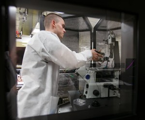
[learn_more caption=”Dr. Hal Evensen (right) and senior Andrew Carlson work in the lab.”]
Watch a YouTube video with Dr. Evensen and Carlson
[/learn_more]
[youtube https://www.youtube.com/watch?v=29kEQj8ZKS8?rel=0&w=400&h=225]
“This laboratory area is for projects from the microsystems and nanotechnology engineering students. This is kind of like their stomping ground,” said Andrew Carlson, a senior physics engineering major from Eau Claire, Wis.
With the completion of Engineering Hall in 2010, one laboratory in particular, under the chemistry and physics department, had plans for conducting education and research, the Nanocharacterization and Materials Fabrication Laboratory.
“Students are using this lab to learn key skill sets they will need in industry,” said Dr. Hal Evensen, professor of engineering physics and program coordinator of microsystems and nanotechnology. “These skill sets are setting them up to contribute to overcoming critical challenges, such as renewable energy, water purification and even new ways to fight disease – all in the lab UW-Platteville is providing them.”
Students majoring in microsystems and nanotechnology engineering frequently use the laboratory. “We use that lab almost every day,” said Greg Seefeldt, a sophomore from Milwaukee, Wis. “After a short lecture, we get the chance to actually fabricate something.”
 Microsystems and nanotechnology classes taught by Dr. Yan Wu, assistant professor in the department of chemistry and engineering physics, learn to make and measure nanoscale materials and learn their use. “In one of my classes I have the students make nanoparticles out of silver and then show them how to kill bacteria using silver nano particles,” said Wu. Silver nano particles are currently in a variety of consumer products as antimicrobial agents. “We also talk about the social and ethical issues of using silver nano particles in consumer products.”
An automatic sliding glass door splits the laboratory into two parts. The entrance to the laboratory is built for classroom purposes, while the other portion of the room is heavily filtered, keeping it as sterile as possible, making it what is known as a “clean,” or low dust room. Without dirty air particles, this allows students and faculty to conduct research.
“Even the classroom portion of the laboratory is a partial clean room,” said Jon Zickermann, a senior from Cedarburg, Wis., majoring in mechanical engineering. “You need a cap, gown and shoe covers to keep it a clean room.”
This laboratory houses state-of-the-art equipment such as an atomic force microscope, used to image and measure nanometer-scale structures; electron microscope to image and measure micrometer-scale structures; and a profilometer to measure thickness of thin films to a resolution of 0.1 nanometer.
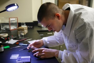 “The research I have been conducting in the last two years is dealing with conduction properties on the nanoscale,” said Carlson.
Carlson’s research requires the use of the atomic force microscope to scan material. He applies a voltage across the material, studies how it conducts and he illuminates it with a laser to look for changes in conduction. “The material may actually work like a solar cell,” said Carlson. Solar cells are the grids that sit on rooftops. They harness the electricity from photons, or light from the sun, to create energy.
“I think laboratories such as the nanocharacterization and materials fabrication laboratory allows undergraduates this amazing hands-on educational opportunity. I think we are extremely fortunate here at UW-Platteville to have access to all of this,” said Carlson.
Written by: Eileen McGuine, UW-Platteville University Information and Communications, (608) 342-1194, mcguinee@uwplatt.edu